The search for flexible, cheap, and easy to process photovoltaic materials took a new turn in the past years with the rapid evolution of organometallic perovskite solar cells. Their high carrier mobility, strong absorption and tunable bandgap make them an ideal candidate for the production of low-cost solar panels.
In order to scale up this technology and compete with silicon panels, a better understanding of perovskite fundamental properties is needed. Photon etc.’s global hyperspectral platforms (IMA and GRAND-EOS) are perfectly suited to find the answers to the questions scientists have been asking themselves about perovskite’s outstanding properties. Indeed, IMA and GRAND-EOS allow rapid characterization of the structural and physical properties of 2D and 3D crystals of perovskite, as well as complete devices. Global hyperspectral imaging combines spectroscopy and imaging; each image is acquired at a narrow band of wavelengths. Spectrally and spatially resolved photoluminescence (PL), electroluminescence (EL), transmittance and reflectance data can be acquired at a high spectral (< 2 nm) and spatial resolution (~µm) over large areas (100 x 100 µm2 – 16 x 16 cm2 or more).
When analysing this combination of spatial and spectral information, it is possible extract information on:
- Absorption
- Presence of defects
- Non-radiative losses
- Homogeneity
- Degradation
When global hyperspectral imaging is combined with Photon etc.’s absolute calibration module, optoelectronics properties can also be extracted:
- Quasi-Fermi level splitting
- Charge transfer efficiency
- Voc
- EQE
Photon etc.’s hyperspectral imager can also be designed for photoluminescence excitation (PLE). PLE is a spectroscopy technique where the excitation wavelength is varied and the luminescence signal is monitored over a fixed broadband emission range. PLE is an efficient technique to study absorption lines of a given material and, when combined with hyperspectral imaging, it provides a useful way to identify inhomogeneities and non-radiative losses.
Photon etc.’s tunable laser source (TLS) is composed of two modules: a supercontinuum source (broadband source) and a laser line tunable filter (LLTF - bandpass filter). When combined with a standard research grade microscope, the TLS can transform the microscope into a hyperspectral PLE setup. This system is continuously tunable in the VIS (400-1000 nm), NIR (900-1620) nm or both (400-1620 nm) spectral ranges. This state of the art platform allows in depth characterisation of advanced materials without any peculiar sample preparation.
Researchers worldwide are using Photon etc.’s hyperspectral imagers to improve their fabrication process.
Perovskite Devices
![Mapping of the current transport efficiency fT calculated from EL hyperspectral images taken at 1.15 V and 1.16 V applied bias. fT mapping was performed at the microscale (top) and at the whole device level (bottom) for perovskite solar cells using PCBM (a, c, device A) or C60 (b, d, device B) as the electron transport layer (ETL). The interpolation of the signal distribution has been overlaid with the color scale as a guide to the eye. Adapted from [1].](https://tj.imgix.net/photonetc/perovskite-spectral-and-spatial-analysis-figure-1.jpg?v=1611600209&w=1200)
Photoluminescence and electroluminescence imaging
Dr. Henk Bolink from the University of Valencia, in collaboration with researchers at IPVF (formerly IRDEP - Institute of Research and Development on Photovoltaic Energy, France), investigated the performance of hybrid organic–inorganic methylammonium lead iodide perovskites (CH3NH3PbI3) solar cells with different electron transport layer (PCBM and C60) [1]. The luminescence hyperspectral data (excitation < 1 sun) obtained with IMA help identify profound inhomogeneities (Fig. 1) in this type of device. “These spatial inhomogeneities appear to be related to problems with carrier extraction, leading to the limited fill factor of the cells.”
Perovskite Crystals
Photoluminescence imaging
Photon etc. collaborated with Prof. David Cooke (McGill University) and Prof Mercouri Kanatzidis (Northwestern University) to study composition of perovskite crystals aged in air. In a few minutes, a million PL spectra were acquired over 550-900 nm spectral range over an area of 670 x 900 µm2 (Fig. 2). Shift in spectral signature and change in intensity were assigned to grain boundaries, defects and phase segregation.


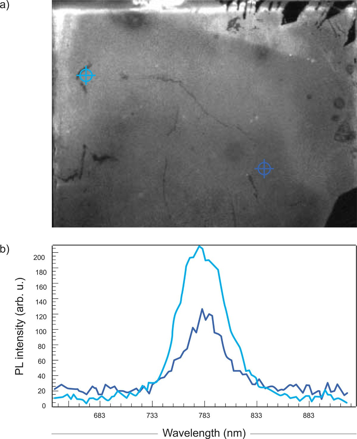
Large perovskite crystals were studied in collaboration with Prof. Pablo Docampo research group (New Castle University). A good solar cell needs to be as luminescent as possible [2]. Mapping of the PL intensity (Fig. 3) provides a rapid way to assess non-radiative losses and get input on a material efficiency. In order to obtain such maps, a 532 nm laser was used to excite the sample at 10 suns equivalent power. Data were acquired in less than a minute from 670 nm to 880 nm with 5 nm steps.

Measurements were also performed on a large scale with Photon etc.’s GRAND-EOS platform. A 532 nm laser was used to excite the sample at 0,1 sun equivalent power. Fig. 4 shows the PL map obtained over a 2 cm x 2 cm field of view. The GRAND-EOS allows capturing the optical picture on a bigger level to help improve the fabrication process.
Photoluminescence excitation imaging
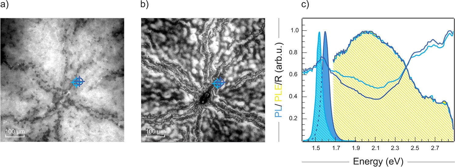
Finally, the same samples were studied with photoluminescence excitation (PLE) and reflectance imaging using Photon etc.’s tunable laser source as the excitation, and PL imaging was performed with Photon etc.’s IMA, with a 532 nm laser excitation source (see figure 5). The PLE spectrum shows that the intensity of the PL emission depends on the energy of the exciting photons with a maximum intensity reached at 2.03 eV excitation. Having access to the spatial information also provides valuable insight on the presence of defects in the sample. It has also been shown that combining PLE with Raman spectroscopy can help identify the origin of PL emission in perovskite crystals. Finally, combining PL and PLE measurements with a Frank-Condon model can provide insight on the electron-phonon interactions [3].

Perovskite Thin Films
![In situ hyperspectral PL maps on the same region for wide-bandgap peaks (a-d) and low-bandgap peaks (e-h) in (Cs0.06MA0.15FA0.79)Pb(Br0.4I0.6)3 perovskite thin films over time under white-light illumination with an intensity of 290 mW/cm² (equivalent to ≈3 suns) for the sample before treatment (t = 0), during the treatment (10 and 30 min), and once the emission intensity reaches stabilized emission (180 min). Maps were taken with 405 nm laser excitation with ≈1 sun intensity (50 mW/cm²) and all measurements were performed in an ambient atmosphere. Adapted from [4].](https://tj.imgix.net/photonetc/perovskite-spectral-and-spatial-analysis-figure-6.jpg?v=1611617395&w=1200)
Photoluminescence imaging
Prof. Sam Stranks (Cambridge University) is studying the fundamental properties of mixed-halide lead perovskites by means of PL imaging (see Fig. 6) [4]. Solution-processed triplecation mixed-halide (Cs0.06MA0.15FA0.79)Pb(Br0.4I0.6)3 perovskite films (MA:methylammonium, FA: formamidinium) are investigated under solar-equivalent illumination. It is found that the illumination leads to localized surface sites of iodide-rich perovskite intermixed with passivating PbI2 material. “This work reveals new insight into phase segregation of mixed-halide mixed-cation perovskites, as well as routes to highly luminescent films by controlling charge density and transfer in novel device structures.”
Other works from Prof. Stranks where hyperspectral imaging was used to characterize perovskite materials:
- Performance-Limiting Nanoscale Trap Clusters at Grain Junctions in Halide Perovskites
- Proton Radiation Hardness of Perovskite Tandem Photovoltaics
- Controlling the Growth Kinetics and Optoelectronic Properties of 2D/3D Lead–Tin Perovskite Heterojunctions
This efficient method provides a deep characterization of perovskite microstructure and will significantly help the understanding of the degradation phenomenon in those materials and bring them one step closer to commercialization.
Photoluminescence excitation imaging
In this work from Rolston et al. [5], PLE hyperspectral imaging was used to study the luminescence yield of perovskite solar cells fabricated with two different processes: open-air rapid spray plasma processing (RSPP) and spin-coating. A tunable laser source from Photon etc. was coupled to a research grade microscope to obtain PLE hyperspectral data. Figure 7 shows PLE spectra (a) extracted from the PLE hyperspectral images (c, e) confirming that the RSPP technique provides higher photoluminescence yield than the spin coated one and is also better suited for fast open-air manufacturing of perovskite solar modules.
![a) Photoluminescence excitation (PLE) spectra of RSPP and spin-coated perovskite b) Optical image and c) corresponding PLE map of spin-coated perovskite compared with d) optical image and e) corresponding PLE map of RSPP perovskite. The higher luminescence from RSPP is observable in both the spectra and the PLE maps. Adapted from [5].](https://tj.imgix.net/photonetc/perovskite-spectral-and-spatial-analysis-figure-7.jpg?v=1611618386&w=1500)
For more information, contact info@photonetc.com
[1] El-Hajje, G., Momblona, C., Gil-Escrig, L., Ávila, J., Guillemot, T., Guillemoles, J.-F., Sessolo, M., Bolink, H. J., & Lombez, L. (2016). Quantification of spatial inhomogeneity in perovskite solar cells by hyperspectral luminescence imaging. Energy & Environmental Science, 9(7), 2286–2294.
[2] Miller, O. D., Yablonovitch, E., & Kurtz, S. R. (2012). Strong Internal and External Luminescence as Solar Cells Approach the Shockley–Queisser Limit. IEEE Journal of Photovoltaics, 2(3), 303–311.
[3] Zelewski, S. J., Urban, J. M., Surrente, A., Maude, D. K., Kuc, A., Schade, L., Johnson, R. D., Dollmann, M., Nayak, P. K., Snaith, H. J., Radaelli, P., Kudrawiec, R., Nicholas, R. J., Plochocka, P., & Baranowski, M. (2019). Revealing the nature of photoluminescence emission in the metal-halide double perovskite Cs2AgBiBr6. Journal of Materials Chemistry C, 7(27), 8350–8356.
[4] Andaji‐Garmaroudi, Z., Abdi‐Jalebi, M., Guo, D., Macpherson, S., Sadhanala, A., Tennyson, E. M., Ruggeri, E., Anaya, M., Galkowski, K., Shivanna, R., Lohmann, K., Frohna, K., Mackowski, S., Savenije, T. J., Friend, R. H., & Stranks, S. D. (2019). A Highly Emissive Surface Layer in Mixed‐Halide Multication Perovskites. Advanced Materials, 31(42), 1902374.
[5] Rolston, N., Scheideler, W. J., Flick, A. C., Chen, J. P., Elmaraghi, H., Sleugh, A., Zhao, O., Woodhouse, M., & Dauskardt, R. H. (2020). Rapid Open-Air Fabrication of Perovskite Solar Modules. Joule.
