Global Hyperspectral Imaging for the Next Generation of Advanced Materials
Conduct your measurements in realistic conditions without damaging your film or device


Upscaling the development of new photovoltaic materials
The field of photovoltaic materials keeps expanding exponentially, and the variety of solar cells has never been so broad. Despite the important advances in this field, newcomers struggle to be economically competitive with silicon-based materials. This is mostly due to the lack of understanding and control over the non-uniformity of the active layers, thus hindering the optimization of optoelectronic properties. In order to bring to the market the next generations of solar cells, researchers have to be able to study the spatial variation of their materials’ properties at a larger scale.
Hyperspectral imaging
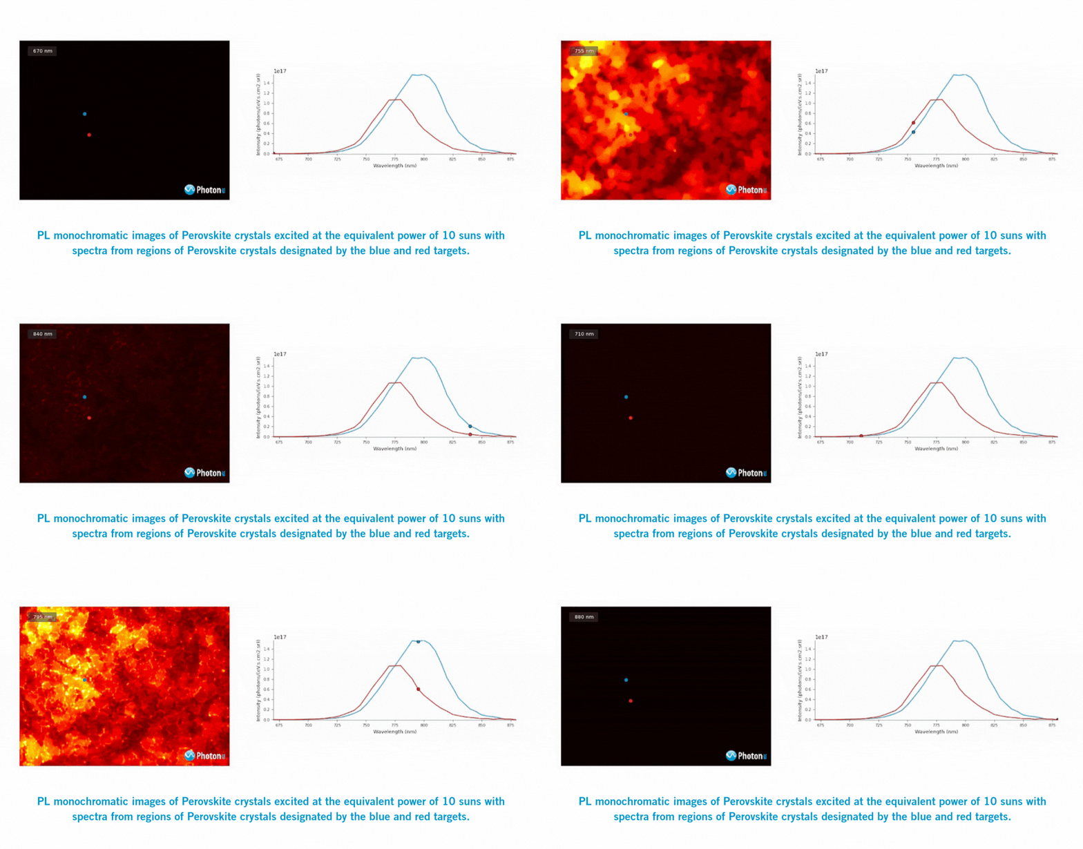
To answer that need, hyperspectral imaging, both macro- and microscopic, provides rapid electroluminescence (EL) and photoluminescence (PL) maps allowing for the spatial observation of defects, constraints, and optoelectronic properties. Those techniques have already been successfully used to characterize inhomogeneities in CIS, CIGS, GAAS and perovskite solar cells.
Absolute photometric calibration
Additionally, absolute photometric calibration provides a direct way to measure the spatial variations of the photoluminescence quantum yield (PLQY), the quasi-Fermi level splitting (Δμ) and the band gap energy (Eg) maps.
Global imaging
Finally, the use of global imaging instead of confocal point-by-point or line-scanning techniques allows for probing the optoelectronic properties in a realistic steady-state, as it reduces the charge diffusion towards darker regions. With uniform illumination, PL experiments are performed in the range of 0.1 suns or up to 500 suns, which are realistic operating conditions of PV panels.

Leverage the Power of Hyperspectral Microscopy : Discover the IMA
IMA is a hyperspectral microscope delivering spectral and spatial information from 400 nm to 1620 nm in one single instrument. By combining a scientific grade VIS, NIR, and/or SWIR microscope with Photon etc patented imaging filter, extensive optical characterization can be achieved on a wide variety of materials. Our hyperspectral imaging microscope is capable of acquiring millions of data points in a single snapshot and rapidly maps photoluminescence (PL), electroluminescence (EL), fluorescence, reflectance, and transmittance. IMA offers the flexibility to be configured as either a brightfield or a darkfield hyperspectral microscope. Moreover, based on high throughput imaging filters, IMA is a faster and more efficient hyperspectral imaging system than standard point-by-point scanning systems.
Photovoltaic Analysis Made Simple : PLQY and QFLS Mapping in Minutes
With the rise of new photovoltaic materials, relying on PLQY mapping alone is no longer enough to evaluate performance. Using data acquired by IMA hyperspectral microscope, our new software module lets you generate essential photovoltaic characterization maps: PLQY, QFLS, and Eg in just a few clicks for deeper, more accurate insights.
Whether you’re just getting started or deep into materials optimization, this tool is fast, reliable, and ready to plug into your solar research workflow.